Complete Summary and Solutions for Semiconductor Electronics: Materials, Devices and Simple Circuits – NCERT Class XII Physics Part II, Chapter 14
semiconductor-electronics-materials-devices-simple-circuits-summary-and-answers-ncert-class-xii-physics-part2-chapter-14
Updated: 7 months ago
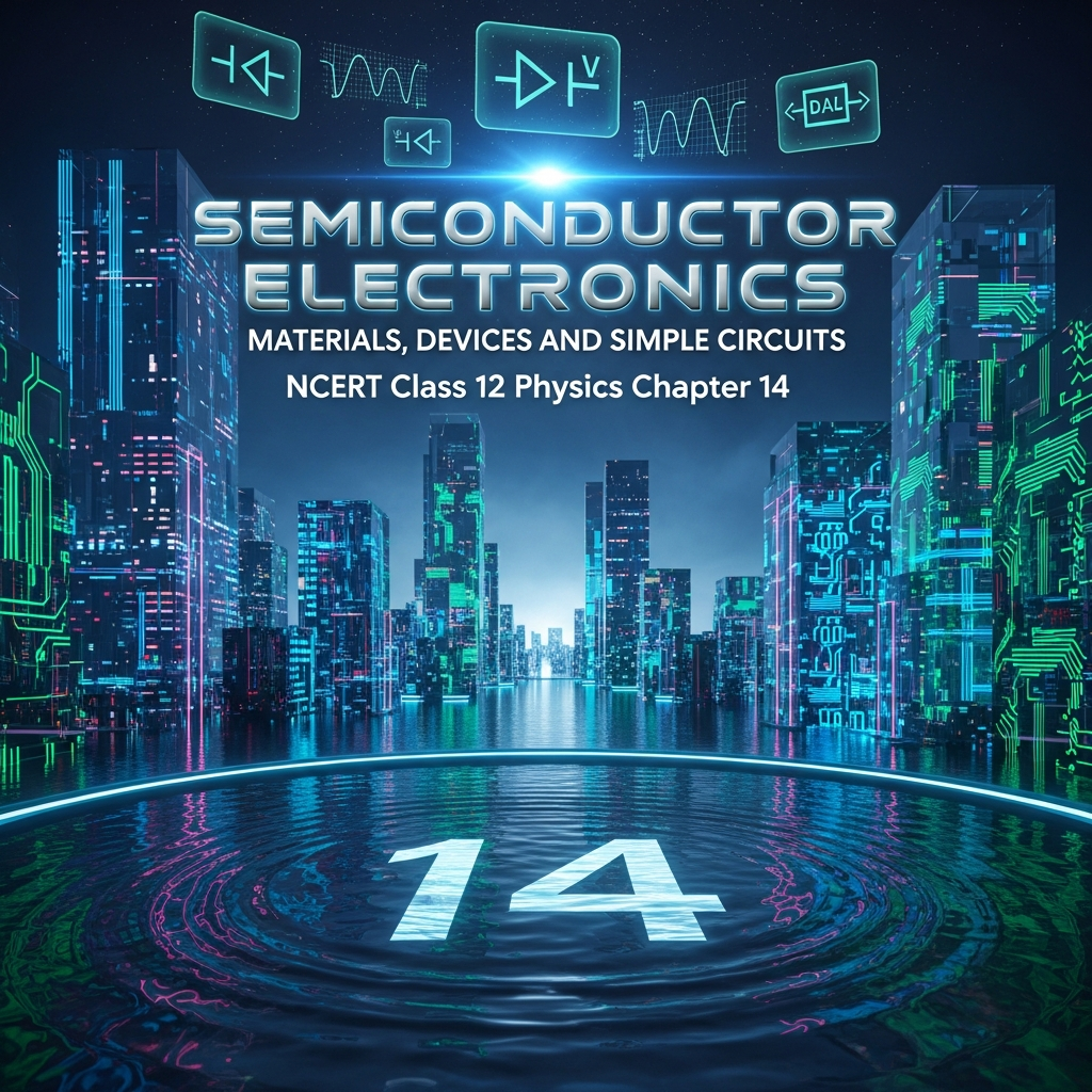
Semiconductor Electronics: Materials, Devices and Simple Circuits
Chapter 14: Physics - Ultimate Study Guide | NCERT Class 12 Notes, Questions, Derivations & Quiz 2025
Full Chapter Summary & Detailed Notes - Semiconductor Electronics Class 12 NCERT
Overview & Key Concepts
- Chapter Goal: Understand semiconductors, doping, diodes, transistors; circuits. Exam Focus: Bands, intrinsic/extrinsic, p-n junction, applications; 2025 Updates: Organic semis, quantum dots. Fun Fact: Transistor 1947. Core Idea: Band gap controls conductivity. Real-World: LEDs, solar cells. Expanded: All subtopics point-wise with evidence (e.g., Fig 14.1 bands), examples (e.g., Si vs Ge Eg), debates (vacuum vs solid-state). Additional: Historical evolution from vacuum tubes to integrated circuits; impact on computing (Moore's Law).
- Wider Scope: From vacuum tubes to modern devices; sources: Text, figures (14.1-14.7), examples. Links to Ch. 3 (current electricity), Ch. 6 (electromagnetic induction for applications).
- Expanded Content: Include resistivity tables, band diagrams; links (e.g., to current electricity Ch3); point-wise breakdown. New: Discussion on compound semiconductors like GaAs for high-speed devices.
Historical Context & Introduction
Pre-1948: Vacuum tubes (diode, triode) bulky, high power. 1930s: Semis control carriers via light/heat/voltage. No heating/vacuum needed. Ex: Galena crystal radio detector. Question: Why Si/Ge over organics? Answer: Si abundance, stable; organics flexible but low mobility. Expanded: Transistor invention by Bardeen, Brattain, Shockley (Nobel 1956); enabled miniaturization.
14.1 Introduction
- Summary in Points: Controlled e- flow: Vacuum tubes (cathode-anode, one-way valves) vs semis (solid-state, low power, reliable). CRT → LCD shift. Semis: Elemental (Si, Ge), compounds (GaAs), organics/polymers. Focus: Inorganic elemental. Expanded: Vacuum tubes: High voltage (~100V), limited life (~1000 hrs); Semis: Room temp, >10^6 hrs life.
- Phenomena: Carrier flow in solid; doping enhances. Additional: Charge carriers: Electrons and holes; mobility μ_e > μ_h.
- Expanded: Evidence: Transistor revolution; debates: Vacuum reliability vs semi life; real: Mobile chips. Additional: Post-1990 polymer electronics birth; e.g., OLEDs in displays.
Conceptual Diagram: Vacuum Tube vs Semiconductor
Heated cathode e- in vacuum vs solid lattice carriers. Evidence: Power consumption contrast (tubes: 10W+, semis: mW). Expanded: Triode: Grid modulates current; equivalent in FETs.
Vacuum Tubes Limitations
- Bulky, ~100V, short life.
- One-way e- flow (valves).
- Example: Triode (grid control). Expanded: Tetrode/pentode reduce secondary emission.
- Additional: Fragile glass envelope; heat dissipation issues.
14.2 Classification of Metals, Conductors and Semiconductors
- Summary in Points: Conductivity basis: Metals (low ρ \(10^{-2}-10^{-8}\) Ωm), Semis (\(10^{-5}-10^6\)), Insulators (\(10^{11}-10^{19}\)). Energy bands: Valence (filled), Conduction (empty); Eg gap. Metals: Overlap/part filled; Insulators: Eg>3eV; Semis: Eg<3eV (Si 1.1eV, Ge 0.7eV). At 0K semis like insulators. Expanded: Conductivity σ = n e μ; n free carriers key.
- Model: Band theory from atomic overlap. Limitations: Ignores doping. Additional: Fermi level E_F in metals at CB bottom.
- Expanded: Evidence: Fig 14.2 bands; debates: Band vs free e-; real: Resistivity measures. Additional: Si/Ge diamond lattice, 4 valence e- → 4N states split to VB (4N filled), CB (4N empty) at 0K. New: Organic semis: Narrow Eg, but low σ.
Diagram: Energy Bands
Fig 14.1: VB filled, CB empty, Eg gap. Fig 14.2: (a) Metal overlap, (b) Insulator large Eg, (c) Semi small Eg. Expanded: At room T, Fermi-Dirac distribution smears occupations.
Band Theory Basics
- Isolated atom: Discrete E. Solid: Overlap → bands. Expanded: Tight-binding model approximates.
- VB: Valence e-; CB: Free conduction. Additional: Forbidden gap Eg from interatomic distance.
- Example: Room T, thermal excitation in semis. New: Direct vs indirect bandgap (Si indirect, GaAs direct for light emission).
14.3 Intrinsic Semiconductor
- Summary in Points: Pure Si/Ge: Covalent bonds (diamond structure). Thermal break bonds → e- (CB) + hole (VB vacancy, +q effective). \( n_e = n_h = n_i \). Holes move via adjacent e- jumps. \( I = I_e + I_h \). Recombination balances generation. Expanded: Generation rate G = recombination R at eq.
- Energy Levels: At T>0K, few e-h pairs; conductivity ↑ with T. Additional: ni ≈ \( 10^{10} \) cm^{-3} for Si at 300K.
- Expanded: Evidence: Fig 14.6 bands at 0K vs T>0; debates: Hole as particle?; real: Temp dependence. Additional: Si lattice a=5.43Å, Ge 5.66Å; Eg Si=1.1eV, Ge=0.7eV. New: Phonon-assisted transitions in indirect semis.
Diagram: e-h Generation
Fig 14.5: Thermal break bond → free e-, hole; hole motion as e- jump. Fig 14.4: 2D covalent net. Expanded: 3D tetrahedral: Each atom 4 bonds, sp^3 hybridization.
Conduction Mechanism
- e- in CB: Negative current. Expanded: Drift velocity v_d = μ E.
- Holes in VB: Apparent + current. Additional: Hole effective mass m_h* > m_e*.
- Ex: At moderate T, few carriers. New: σ_i = e ni (μ_e + μ_h).
14.4 Extrinsic Semiconductor
- Summary in Points: Low room T conductivity → doping (ppm impurities). Dopants: Pentavalent (As,P: n-type, donor e-); Trivalent (B,In: p-type, acceptor hole). n-type: ne >> nh; p-type: nh >> ne. Size match dopant-host. Expanded: Doping concentration Nd ~10^{15}-10^{18} cm^{-3}.
- Doping Effects: Extra carriers, low ionization E (~0.05eV Si). Additional: Impurity levels: Donor E_d ≈ 0.045 eV below EC.
- Expanded: Evidence: Fig 14.7 n-type; debates: Intrinsic vs extrinsic; real: Device fabrication. Additional: Donor ionization >> intrinsic at room T. New: Compensation doping (n + p-type impurities).
n-type Doping
- Pentavalent: 4 bonds, 1 free e-. Expanded: As atomic radius 1.18Å ≈ Si 1.11Å.
- ne = donors + intrinsic; nh ↓ recombination. Additional: Law of mass action: ne nh = ni^2.
- Example: P in Si. New: Hall effect measures carrier type.
p-type Doping
- Trivalent: 3 bonds, 1 hole. Expanded: B in Si: Acceptor level E_a ≈ 0.045 eV above EV.
- nh ≈ Na; ne ↓. Additional: Ionized acceptor Na^- fixed negative charge.
- Example: In in Ge. New: Applications in BJT base.
14.5 p-n Junction (Expanded from Chapter)
- Summary: Diffusion: Holes to n-side, e- to p-side → depletion region, barrier V_bi ≈ 0.7V Si. Forward bias: Reduces barrier, current ↑ exp(V/V_T). Reverse: Increases, small leakage. Expanded: V_bi = (kT/q) ln(Na Nd / ni^2).
Diagram: p-n Junction
Depletion width W ∝ sqrt(V_bi - V). I-V: Exponential forward.
14.6 Applications: Diode, LED, Zener
- Rectifier, clipper; LED: Recombination light; Zener breakdown. Expanded: Photodiode: Reverse bias photocurrent.
14.7 Transistor (BJT)
- npn/pnp; CE config β = Ic/Ib. Expanded: Regions: Active, saturation, cutoff.
14.8 Logic Gates
- AND, OR, NOT from diodes/transistors. Expanded: Truth tables, Boolean algebra.
Summary (From PDF)
- Vacuum → semis revolution. Bands classify materials. Intrinsic: e-h thermal. Extrinsic: Doping majority carriers. Full Chapter: Junctions enable rectification; transistors amplification; gates digital logic.
- Focus: Si/Ge; later chapters: Junctions, devices. Exam Weight: 8-10 marks.
Points to Ponder (From PDF)
- Why vacuum? Collision-free e- path.
- Band overlap in metals: Free e-.
- Hole motion: Collective bound e- shift.
- Doping: Impurity levels near band edges.
- Recombination: e- + hole → bond. Additional: Radiative/non-radiative.
- Junction barrier: Built-in field E = V_bi / W.
Key Themes & Tips
- Aspects: Bands, carriers, doping, junctions. Expanded: Quantum wells in modern devices.
- Tip: Sketch bands; compare intrinsic/extrinsic; memorize Eg, ρ ranges. Exam: Conceptual on holes, numerical on doping effects, I-V curves.
Project & Group Ideas
- Build simple diode circuit. Expanded: Half-wave rectifier with LED load.
- Debate: Si vs GaAs for LEDs. Additional: Cost vs efficiency.
- Simulate band diagrams (PhET). New: Use Python/Matlab for ni(T).
- Group: Measure resistivity vs T. Expanded: Four-probe method.


As an Amazon Associate, ProSyllabus earns from qualifying purchases. Prices shown are subject to change.
Test your CBSE Class 12 Board Examination prep
Quizzes
10 questions · ~10 minutes · instant rank & AI diagnosis
Economics (Class 12) Practice Quiz | CBSE Class 12 Board Examination
Accountancy (Class 12) Practice Quiz | CBSE Class 12 Board Examination
Electrostatic Potential and Capacitance Fundamentals | CBSE Class 12 Board Examination
Class 12 English — Memories of Childhood (Practice Quiz)
Class 12 English — On the Face of It (Practice Quiz)
Class 12 English — The Enemy (Practice Quiz)
Class 12 English — Journey to the End of the Earth (Practice Quiz)
Class 12 English — The Tiger King (Practice Quiz)
Class 12 English — The Third Level (Practice Quiz)
Class 12 English — Aunt Jennifer's Tigers (Practice Quiz)
Class 12 English — A Roadside Stand (Practice Quiz)
Class 12 English — A Thing of Beauty (Practice Quiz)
Class 12 English — Keeping Quiet (Practice Quiz)
Class 12 English — An Elementary School Classroom in a Slum (Practice Quiz)
Class 12 English — My Mother at Sixty-six (Practice Quiz)
Class 12 English — Going Places (Practice Quiz)
Class 12 English — The Interview (Practice Quiz)
Class 12 English — Poets and Pancakes (Practice Quiz)
Class 12 English — Indigo (Practice Quiz)
Class 12 English — The Rattrap (Practice Quiz)
Class 12 English — Deep Water (Practice Quiz)
Class 12 English — Lost Spring (Practice Quiz)
Class 12 English — The Last Lesson (Practice Quiz)
Class 12 Psychology — Social Influence and Group Processes (Practice Quiz)
Class 12 Psychology — Attitude and Social Cognition (Practice Quiz)
Class 12 Psychology — Therapeutic Approaches (Practice Quiz)
Class 12 Psychology — Psychological Disorders (Practice Quiz)
Class 12 Psychology — Meeting Life Challenges (Practice Quiz)
Class 12 Psychology — Self and Personality (Practice Quiz)
Class 12 Psychology — Variations in Psychological Attributes (Practice Quiz)
Class 12 Sociology — Social Movements (Practice Quiz)
Class 12 Sociology — Mass Media and Communications (Practice Quiz)
Class 12 Sociology — Globalisation and Social Change (Practice Quiz)
Class 12 Sociology — Change and Development in Industrial Society (Practice Quiz)
Class 12 Sociology — Change and Development in Rural Society (Practice Quiz)
Class 12 Sociology — The Constitution and Social Change (Practice Quiz)
Class 12 Sociology — Cultural Change (Practice Quiz)
Class 12 Sociology — Structural Change (Practice Quiz)
Class 12 Sociology — The Challenges of Cultural Diversity (Practice Quiz)
Class 12 Sociology — Patterns of Social Inequality and Exclusion (Practice Quiz)
Class 12 Sociology — The Market as a Social Institution (Practice Quiz)
Class 12 Sociology — Social Institutions: Continuity and Change (Practice Quiz)
Class 12 Sociology — The Demographic Structure of the Indian Society (Practice Quiz)
Class 12 Sociology — Introducing Indian Society (Practice Quiz)
Class 12 Political Science — Recent Developments in Indian Politics (Practice Quiz)
Class 12 Political Science — Regional Aspirations (Practice Quiz)
Class 12 Political Science — The Crisis of Democratic Order (Practice Quiz)
Class 12 Political Science — Challenges to and Restoration of the Congress System (Practice Quiz)
Class 12 Political Science — India's External Relations (Practice Quiz)
Class 12 Political Science — Politics of Planned Development (Practice Quiz)
Class 12 Political Science — Era of One-party Dominance (Practice Quiz)
Class 12 Political Science — Challenges of Nation Building (Practice Quiz)
Class 12 Political Science — Environment and Natural Resources (Practice Quiz)
Class 12 Political Science — Security in the Contemporary World (Practice Quiz)
Class 12 Political Science — International Organisations (Practice Quiz)
Class 12 Political Science — Contemporary South Asia (Practice Quiz)
Class 12 Political Science — Contemporary Centres of Power (Practice Quiz)
Class 12 Political Science — The End of Bipolarity (Practice Quiz)
Class 12 Geography — Geographical Perspective on Selected Issues and Problems (Practice Quiz)
Class 12 Geography — Planning and Sustainable Development in the Indian Context (Practice Quiz)
Class 12 Geography — Mineral and Energy Resources (Practice Quiz)
Class 12 Geography — Water Resources (Practice Quiz)
Class 12 Geography — Land Resources and Agriculture (Practice Quiz)
Class 12 Geography — Human Settlements (Practice Quiz)
Class 12 Geography — Population: Distribution, Density, Growth and Composition (Practice Quiz)
Class 12 Geography — International Trade (India) (Practice Quiz)
Class 12 Geography — Transport and Communication (India) (Practice Quiz)
Class 12 Geography — Tertiary and Quaternary Activities (Practice Quiz)
Class 12 Geography — Secondary Activities (Practice Quiz)
Class 12 Geography — Primary Activities (Practice Quiz)
Class 12 Geography — Human Development (Practice Quiz)
Class 12 Geography — The World Population: Distribution, Density and Growth (Practice Quiz)
Class 12 Geography — Human Geography: Nature and Scope (Practice Quiz)
Class 12 History — Framing the Constitution — The Beginning of a New Era (Practice Quiz)
Class 12 History — Mahatma Gandhi and the Nationalist Movement — Civil Disobedience and Beyond (Practice Quiz)
Class 12 History — Rebels and the Raj — The Revolt of 1857 and its Representations (Practice Quiz)
Class 12 History — Colonialism and the Countryside — Exploring Official Archives (Practice Quiz)
Class 12 History — Peasants, Zamindars and the State — Agrarian Society and the Mughal Empire (c. sixteenth-seventeenth centuries) (Practice Quiz)
Class 12 History — An Imperial Capital: Vijayanagara (c. fourteenth to sixteenth century) (Practice Quiz)
Class 12 History — Bhakti-Sufi Traditions — Changes in Religious Beliefs and Devotional Texts (c. eighth to eighteenth century) (Practice Quiz)
Class 12 History — Through the Eyes of Travellers — Perceptions of Society (c. tenth to seventeenth century) (Practice Quiz)
Class 12 History — Thinkers, Beliefs and Buildings — Cultural Developments (c. 600 BCE-600 CE) (Practice Quiz)
Class 12 History — Kinship, Caste and Class — Early Societies (c. 600 BCE-600 CE) (Practice Quiz)
Class 12 History — Kings, Farmers and Towns — Early States and Economies (c. 600 BCE-600 CE) (Practice Quiz)
Class 12 History — Bricks, Beads and Bones — The Harappan Civilisation (Practice Quiz)
Class 12 Economics — Open Economy Macroeconomics (Practice Quiz)
Class 12 Economics — Government Budget and the Economy (Practice Quiz)
Class 12 Economics — Determination of Income and Employment (Practice Quiz)
Class 12 Economics — Money and Banking (Practice Quiz)
Class 12 Economics — National Income Accounting (Practice Quiz)
Class 12 Economics — Market Equilibrium (Practice Quiz)
Class 12 Economics — The Theory of the Firm under Perfect Competition (Practice Quiz)
Class 12 Economics — Production and Costs (Practice Quiz)
Class 12 Economics — Theory of Consumer Behaviour (Practice Quiz)
Class 12 Economics — Introduction (Practice Quiz)
Class 12 Business Studies — Consumer Protection (Practice Quiz)
Class 12 Business Studies — Marketing (Practice Quiz)
Class 12 Business Studies — Financial Management (Practice Quiz)
Class 12 Business Studies — Controlling (Practice Quiz)
Class 12 Business Studies — Directing (Practice Quiz)
Class 12 Business Studies — Staffing (Practice Quiz)
Class 12 Business Studies — Organising (Practice Quiz)
Class 12 Business Studies — Planning (Practice Quiz)
Class 12 Business Studies — Business Environment (Practice Quiz)
Class 12 Business Studies — Nature and Significance of Management (Practice Quiz)
Class 12 Accountancy — Cash Flow Statement (Practice Quiz)
Class 12 Accountancy — Accounting Ratios (Practice Quiz)
Class 12 Accountancy — Analysis of Financial Statements (Practice Quiz)
Class 12 Accountancy — Financial Statements of a Company (Practice Quiz)
Class 12 Accountancy — Issue and Redemption of Debentures (Practice Quiz)
Class 12 Accountancy — Accounting for Share Capital (Practice Quiz)
Class 12 Accountancy — Dissolution of Partnership Firm (Practice Quiz)
Class 12 Accountancy — Reconstitution of a Partnership Firm – Retirement/Death of a Partner (Practice Quiz)
Class 12 Accountancy — Reconstitution of a Partnership Firm – Admission of a Partner (Practice Quiz)
Class 12 Accountancy — Accounting for Partnership: Basic Concepts (Practice Quiz)
Class 12 Maths — Probability (Practice Quiz)
Class 12 Maths — Linear Programming (Practice Quiz)
Class 12 Maths — Three Dimensional Geometry (Practice Quiz)
Class 12 Maths — Vector Algebra (Practice Quiz)
Class 12 Maths — Differential Equations (Practice Quiz)
Class 12 Maths — Application of Integrals (Practice Quiz)
Class 12 Maths — Integrals (Practice Quiz)
Class 12 Maths — Application of Derivatives (Practice Quiz)
Class 12 Maths — Continuity and Differentiability (Practice Quiz)
Class 12 Maths — Determinants (Practice Quiz)
Class 12 Maths — Matrices (Practice Quiz)
Class 12 Maths — Inverse Trigonometric Functions (Practice Quiz)
Class 12 Maths — Relations and Functions (Practice Quiz)
Class 12 Biology — Biodiversity and its Conservation (Practice Quiz)
Class 12 Biology — Ecosystem (Practice Quiz)
Class 12 Biology — Organisms and Populations (Practice Quiz)
Class 12 Biology — Biotechnology and its Applications (Practice Quiz)
Class 12 Biology — Biotechnology: Principles and Processes (Practice Quiz)
Class 12 Biology — Microbes in Human Welfare (Practice Quiz)
Class 12 Biology — Human Health and Disease (Practice Quiz)
Class 12 Biology — Evolution (Practice Quiz)
Class 12 Biology — Molecular Basis of Inheritance (Practice Quiz)
Class 12 Biology — Principles of Inheritance and Variation (Practice Quiz)
Class 12 Biology — Reproductive Health (Practice Quiz)
Class 12 Biology — Human Reproduction (Practice Quiz)
Class 12 Biology — Sexual Reproduction in Flowering Plants (Practice Quiz)
Class 12 Chemistry — Biomolecules (Practice Quiz)
Class 12 Chemistry — Amines (Practice Quiz)
Class 12 Chemistry — Aldehydes, Ketones and Carboxylic Acids (Practice Quiz)
Class 12 Chemistry — Alcohols, Phenols and Ethers (Practice Quiz)
Class 12 Chemistry — Haloalkanes and Haloarenes (Practice Quiz)
Class 12 Chemistry — Coordination Compounds (Practice Quiz)
Class 12 Chemistry — The d- and f-Block Elements (Practice Quiz)
Class 12 Chemistry — Chemical Kinetics (Practice Quiz)
Class 12 Chemistry — Electrochemistry (Practice Quiz)
Class 12 Chemistry — Solutions (Practice Quiz)
Class 12 Physics — Semiconductor Electronics: Materials, Devices and Simple Circuits (Practice Quiz)
Class 12 Physics — Nuclei (Practice Quiz)
Class 12 Physics — Atoms (Practice Quiz)
Class 12 Physics — Dual Nature of Radiation and Matter (Practice Quiz)
Class 12 Physics — Wave Optics (Practice Quiz)
Class 12 Physics — Ray Optics and Optical Instruments (Practice Quiz)
Class 12 Physics — Electromagnetic Waves (Practice Quiz)
Class 12 Physics — Alternating Current (Practice Quiz)
Class 12 Physics — Electromagnetic Induction (Practice Quiz)
Class 12 Physics — Magnetism and Matter (Practice Quiz)
Class 12 Physics — Moving Charges and Magnetism (Practice Quiz)
Class 12 Physics — Electrostatic Potential and Capacitance (Practice Quiz)
Class 12 Physics — Electric Charges and Fields (Practice Quiz)
Class 12 Business Studies — Principles of Management (Practice Quiz)
CBSE Class 12 — Genetics and Evolution (Practice Quiz)
CBSE Class 12 — Matrices and Determinants (Practice Quiz)
CBSE Class 12 — Solutions and Colligative Properties (Practice Quiz)
Class 12 Physics — Current Electricity (Practice Quiz)
CBSE Class 12 — Electrostatics and Electric Field (Practice Quiz)
Humanities Subjects Practice Quiz | CBSE Class 12 Board Examination

Group Discussions
No forum posts available.

